A06, an undergraduate class that provides students hands-on experience in nano fabrication making use of the toolsets and cleanroom of MIT.nano, first-year undergraduate Audrey Lee loads an electron-beam evaporator with silicon wafers, a procedure action in the development of a solar cell. Theyre also getting an experience not typical at the undergraduate level– gowning up in a bunny match and performing hands-on research inside a tidy room.During the fall 2021 semester, these students were part of 6.,” an encouraging workshop for first-year students, had comparable goals: showing undergrads whats possible at the nanoscale through hands-on clean-room experiences. And, with experience working in a particle-free environment, Scholvin states, these students are now prepared for future opportunities, such as carrying out nanoscale research with faculty through the Undergraduate Research Opportunities Program.
The occasion, which brings together over 200 trainees, faculty, and industry partners to celebrate scientific advances in nanotechnology, traditionally includes discussions by graduate-level trainees.
In 6. A06, an undergraduate class that offers students hands-on experience in nano fabrication using the toolsets and cleanroom of MIT.nano, first-year undergraduate Audrey Lee loads an electron-beam evaporator with silicon wafers, a process action in the development of a solar cell. Credit: Jesus del AlamoUndergraduate classes supply hands-on introduction to nanotechnology and nanoengineering at MIT.nano.MIT undergraduates are using labs at MIT.nano to tinker at the nanoscale, checking out spectrometry, nanomaterial synthesis, photovoltaics, sensor fabrication, and other topics. Theyre likewise getting an experience not common at the undergraduate level– gowning up in a bunny match and carrying out hands-on research study inside a tidy room.During the fall 2021 term, these students were part of 6. S059 (Nanotechnology– Design From Atoms to Everything) and 6. A06 (First.nano!– Fabricate Your Own Solar Cell in MIT.nano Cleanroom), two classes offered by the Department of Electrical Engineering and Computer Science (EECS) intended at introducing undergraduates to nanoscience through design-focused knowing utilizing appropriate fabrication processes and tool sets.” Classes like these can be transformational experiences for our students,” says MIT.nano Director Vladimir Bulovic, the Fariborz Maseeh (1990) Chair in Emerging Technology. “They spread the message that nanoscience is at your fingertips. Its not some far-off, abstract idea, however accessible here and now. We are enjoyed see MIT professors motivating and shaping the future leaders of science and innovation by showing them what they can master inside MIT.nano.”
Utilizing easy tools to encourage broad exploration
Class 6. S059 was established to bridge the basics of engineering style with the real building of functional incorporated innovations, something normally separated into numerous classes and terms.
Over 9 weeks, 18 students from 5 different scholastic departments found out a number of nanoscale prototyping methods in MIT.nano including spin covering, maskless lithography, 3D printing, colloidal synthesis, sputtering, evaporation, and optical microscopy. By concentrating on a variety of basic tools, the students could do much of the work without needing extensive, specific training. Instead of watching mentor assistants run devices, these undergraduates might do the research themselves and, in the procedure, focus on how the science works, rather than how to run a complex setup.
Left to right: Mechanical engineering junior Sophia Sonnert, EECS senior Sidne Gregory, and EECS senior Veronica Grant display their 6. The group printed their names and the MIT seal on flexible subtrates utilizing fluorescent ink and the tools of MIT.nano.
” We wanted to teach the science of what you require to create nanodevices and systems in an interactive and hands-on way,” states co-instructor Farnaz Niroui, the EE Landsman (1958) Career Development Assistant Professor of Electrical Engineering and Computer Science at MIT. “Often, these initial courses take on a heavy mathematical/theoretical approach, which can make it tough to preserve students interest. We decided to teach it through an applied approach– having the trainees design and develop, while finding out the principles along the method.”
Rather of giving directions on how to do each step in weekly labs, Niroui and co-instructor Rajeev Ram, teacher of electrical engineering, taught the end result (such as using light to observe things you can not see with the naked eye) and after that let the trainees explore putting together the tool set required to get there (such as designing and constructing their portable spectrometers and own microscopes). Every weeks job developed on the one before. For example, the undergraduates initially designed their own spectrometers, then produced the optical grating and a 3D printed case to assemble the tool. This resulted in a hands-on introduction to CAD photolithography, design, and 3d printing, followed by having fun with various lights and testing their devices on real-world applications by measuring the chlorophyll in a leaf and the emission of quantum dots.
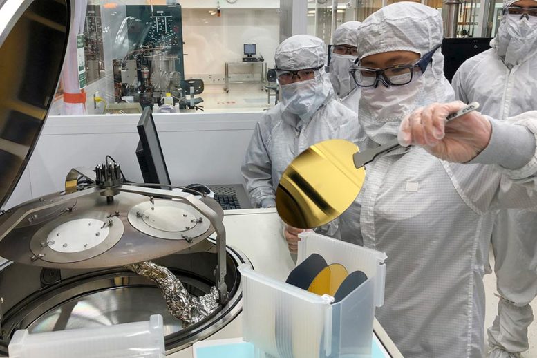
A student loads the PicoTrack, a fully automated coat-and-develop track system for spin coating, spray establishing, and puddle developing of 6-inch and 8-inch wafers. Credit: Jesus del Alamo
For their last job, the students divided into teams to create and develop their own operating gadgets. Each task had to utilize products and techniques covered in the class, and have at least one feature smaller than 100 nanometers. All six groups were eventually effective, conquering obstacles to develop elastic sensors utilizing silver nanowires, seven-segment pixelated display screens for wearable applications, a programmable natural light-emitting diode matrix, light-trapping microstructures for thin-film solar cells, color-tunable light-emitting diode, and printing fluorescent ink on versatile substrates.
” Seeing the students style and construct their own gadgets after just a few weeks of guideline was outstanding and amazing,” says Ram. “It showed that hands-on intro to sophisticated ideas in physics can actually supply undergrads with useful, working understanding about nanotechnology.”
6. S059 student Syamantak Payra, a senior from the Department of Electrical Engineering and Computer Science, displays his teams seven-segment pixelated screen. The group made an organic light-emitting diode and then incorporated it to a working circuit (which they likewise developed) to output temperature level sensing unit readings. Credit: Thomas Gearty
This was the first year for the design-focused nanotechnology class. Niroui and Ram hope to scale it up in future semesters, broadening the offering to more undergrads.
” Many of the trainees have actually stated they are thrilled to explore even more into the world of used science and hardware engineering,” states mentor assistant Mayuran Saravanapavanantham, a PhD candidate in EECS. “One even said they browsed MITs course listings for anything with the term nano.” Saravanapavanantham was among 3 TAs for 6. S059, together with Roberto Brenes and Peter Satterthwaite, all EECS doctoral students.
An early look into the nanoworld
,” an encouraging workshop for first-year trainees, had similar goals: revealing undergrads whats possible at the nanoscale through hands-on clean-room experiences. For 3 hours each week, MIT students in 6.
” How do we get first-year students interested in nanofabrication?” asks Jorg Scholvin. “Bring them into the tidy space and let them discover by doing things in the laboratory.” The method absolutely triggered interest: More than 30 inbound undergraduates applied to fill one of the 8 slots provided in the seminar.
Students do not typically enter the clean space during their undergraduate research studies, states Scholvin. By presenting them to nanofabrication in their first semester, del Alamo and Scholvin want to accelerate their courses into nano-related fields. And, with experience working in a particle-free environment, Scholvin says, these trainees are now prepared for future chances, such as performing nanoscale research study with faculty through the Undergraduate Research Opportunities Program.
“MIT.nano is an extraordinary center. By creating opportunities for these trainees to work and study here, we hope to open it up to broad usage for undergraduate research study and education.”
Undergraduates from both 6. The occasion, which brings together over 200 trainees, professors, and market partners to commemorate scientific advances in nanotechnology, traditionally includes discussions by graduate-level students.