
A Q&A with 2 researchers intending to conquer limitations in calculating power and energy efficiency by creating brand-new microchips.
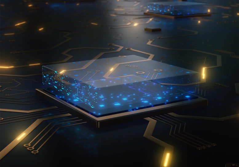
Our smart devices and laptop computers are compact yet powerful due to the fact that of silicon microelectronics, likewise referred to as microchips or chips, the small brains behind the digital brawn of almost every contemporary gadget.
Such modern convenience comes at a cost. By 2030, about 25% of the worlds energy– most of which is produced by burning carbon-rich nonrenewable fuel sources– could be consumed by electronic gadgets if absolutely nothing is done to make them more energy effective.
Silicon chips stem from a style known as CMOS, shorthand for complementary metal-oxide-semiconductor. As Moores Law initially predicted in 1975, CMOS silicon chips are approaching limits in miniaturization and performance. For decades, scientists have been on the hunt for brand-new electronic products that exceed the limits of Moores Law in addition to the restrictions of silicon CMOS chips.
Now, researchers Maurice Garcia-Sciveres and Ramamoorthy Ramesh at DOEs Lawrence Berkeley National Laboratory (Berkeley Lab) are creating new microchips that might perform much better– and require less energy– than silicon. Over the next 3 years, they will lead 2 of the 10 tasks recently awarded almost $54 million by the Department of Energy to increase energy efficiency in microelectronics design and production.
They discuss their projects in this Q&A.
Berkeley Lab scientists Maurice Garcia-Sciveres (left) and Ramamoorthy Ramesh are designing new microchips that could perform better– and require less energy– than silicon. Credit: Courtesy of Garcia-Sciveres and Ramesh
Q: Over the next 3 years, what do you want to achieve? What is the significance of your work?.
Garcia-Sciveres: Our project– the “Co-Design and Integration of Nano-Sensors on CMOS”– intends to improve efficiency by integrating small light sensing units made with nanomaterials into a conventional CMOS (complementary metal-oxide-semiconductor) integrated circuit. (A nanomaterial is matter designed at an ultrasmall scale of a billionth of a meter.).
CMOS chips are made of silicon, however if you look at how much power silicon utilizes, its beginning to be significant– and in a years, silicon chips will be taking in a big portion of our energy. The computing required to run a self-driving automobile consumes substantial energy compared to the energy needed to run the cars and truck. We need to calculate with less energy, or boost efficiency without more power, however you cant do that with silicon chips since silicon needs to run on a specific voltage– and those physical restrictions are costing us.
In our task, nanomaterials such as carbon nanotubes– gadgets so little that they are invisible to the naked eye– would function as light sensing units. The nanosensors include new performance to a CMOS chip, increasing performance.
Noticing is a great initial application, however when incorporated into a chip, the carbon nanotubes might likewise work as transistors or switches that process data. Incorporating many carbon nanotubes into a silicon chip could cause new kinds of electronic devices that are smaller sized and much faster along with more energy efficient than existing technologies.
Ramesh: In our task, “Co-Design of Ultra-Low-Voltage Beyond CMOS Microelectronics,” we plan to check out brand-new physical phenomena that will lead to significantly greater energy efficiency in computing. This is important since our company believe that the next Moores Law is most likely to be concentrated on the energy scale and not the length scale, given that we are already at the limitations of length scaling.
In around 2015, energy consumption from microelectronics was only about 4-5% of the worlds overall primary energy. Main energy usually suggests the chemical energy produced by a coal- or natural gas-based power plant. This usually has a performance of conversion to electrical energy of 35-40%.
Our increasing reliance on expert system, maker knowing, and IoT– or the Internet of Things where everything is digitally linked, such as our traffic systems, emergency action systems, and renewable resource and electrical grid systems– will lead to an exponential boost of electronics from the systems perspective.
This means that by 2030, energy intake from microelectronics is projected to be a minimum of 25% of primary energy. Making electronics more energy effective is a big offer.
For our task, we are asking, “What basic materials developments could significantly scale back the energy usage of microelectronics?” Were taking a look at a completely various structure that checks out brand-new physics using a co-design approach, in which world-leading specialists in products physics, gadget and circuit fabrication, screening and design, and chip-level architecture are operating in partnership to perform a holistic research study of paths to next-generation computing.
Q: What brand-new applications will your work enable, and how will you demonstrate these new abilities?.
Garcia-Sciveres: Our work will show a single-photon imager that can measure the spectrum– the wavelength or energy– of each and every single photon or light particle it identifies. This permits hyperspectral imaging– that is, images where each pixel can be decayed into numerous colors, providing a lot more details. Hyperspectral imaging advantages a broad variety of science, from cosmology to biological imaging.
The Dark Energy Spectroscopic Experiment (DESI), an international science partnership handled by Berkeley Lab, captures the spectra of distant galaxies, beginning with images of the galaxies that were formerly taken with other instruments. This included spectral details helps cosmologists understand how dark energy formed the expansion of our universe. Had the original observations of the galaxies been made with a hyperspectral imager, spectral info would have been available to begin with.
Another growing application of hyperspectral imaging is the research study of exoplanets. (Planets in our planetary system orbit around the Sun. Worlds that orbit around other stars are called exoplanets.).
The sensors utilized for these types of observations work at temperature levels less than 1 degree above absolute zero. Our gadget would operate at more practical temperature levels, possibly even up to room temperature.
Hyperspectral imaging has many applications in medicine and biosciences, and lots of industrial instruments are readily available. These instruments, which are all much more complex and more expensive than a routine video camera, either scan an item pixel by pixel or have complex plans of robotic fibers or filters. These instruments do not have single-photon level of sensitivity. Our device would make it possible for an easy cam that supplies hyperspectral images with single-photon level of sensitivity.
Ramesh: Our team is designed to show the practicality and power of our co-design platform, “Atoms to Architecture,” which is built upon 2 basic physical phenomena:.
The first is an unique behavior in ferroelectric-based transistor architectures that provides a pathway to lower the total energy consumed in a silicon-based microelectronics device. (A ferroelectric is a product with an electrical dipole — or a set of unfavorable and favorable electrical charges– that is switchable with an electrical field.) The 2nd is the low-voltage electric field control of electronic spin utilizing a novel class of materials called multiferroics.
In 2014, we demonstrated a magneto-electric material that can convert charge into magnetic spin at 5 volts of used voltage. Subsequent collaborative work with scientists at Intel demonstrated how this might be utilized to produce a new class of logic-in-memory gadgets, termed the MESO gadget, which utilizes spins to carry out logic operations.
For one of our tasks within our program, we will use our magneto-electric material to explore multiferroic aspects that will function at 100 millivolts, resulting in a substantial drop in energy consumption. (A millivolt is one thousandth of a volt.).
Our second task is checking out the essential physics of a capacitor device, in which a ferroelectric layer is overlaid on a standard silicon transistor to improve its energy effectiveness through whats called the negative capacitance effect. Our style would make it possible for a microelectronics gadget that carries out both memory and reasoning functions– This technique is significantly various from the chips in our computers today, where one type of chip performs the reasoning or processing of data, and another chip stores information.
The “Co-Design and Integration of Nano-Sensors on CMOS” job is a cooperation in between researchers at Berkeley Lab, Sandia National Laboratory, and UC Berkeley. Co-principal private investigators include Weilun Chao, Steve Holland, Mi-Young Im, Tevye Kuykendall, Francois Leonard, Yuan Mei, Andrew Nonaka, Katerina Papadopoulou, Greg Tikhomoirov, Archana Raja, Ricardo Ruiz, and Jackie Yao.
The “Co-Design of Ultra-Low-Voltage Beyond CMOS Microelectronics task” is a collaboration between researchers at Berkeley Lab and UC Berkeley. Co-principal private investigators consist of Sinéad Griffin, Lane Martin, Lavanya Ramakrishnan, Sayeef Saluhuddin, Padraic Shafer, John Shalf, Dilip Vasudevan, and Jackie Yao.
CMOS chips are made of silicon, however if you look at how much power silicon utilizes, its beginning to be considerable– and in a decade, silicon chips will be consuming a large fraction of our energy. The computing needed to run a self-driving automobile takes in significant energy compared to the energy required to run the vehicle. We need to calculate with less energy, or boost efficiency without more power, but you cant do that with silicon chips due to the fact that silicon has to run on a particular voltage– and those physical limitations are costing us.
In around 2015, energy usage from microelectronics was just about 4-5% of the worlds overall primary energy. Primary energy generally indicates the chemical energy produced by a coal- or natural gas-based power plant.