Human beings experience the world in 3 dimensions, but a collaboration in Japan has actually developed a way to produce synthetic measurements to much better understand the fundamental laws of the Universe and potentially use them to innovative innovations.
They released their outcomes today (January 28, 2022) in Science Advances.
” The concept of dimensionality has ended up being a central component in diverse fields of contemporary physics and technology in previous years,” said paper author Toshihiko Baba, teacher in the Department of Electrical and Computer Engineering, Yokohama National University. “While queries into lower-dimensional products and structures have actually been productive, rapid advances in geography have uncovered an additional abundance of potentially helpful phenomena depending on the dimensionality of the system, even surpassing the three spatial dimensions available in the world around us.”
Geography describes an extension of geometry that mathematically describes areas with properties maintained in constant distortion, such as the twist of a mobius strip. When integrated with light, according to Baba, these physical areas can be directed in a method that enables researchers to induce extremely made complex phenomena.
In the real world, from a line to a square to a cube, each measurement provides more details, too needs more knowledge to properly explain it. In topological photonics, scientists can develop extra measurements of a system, enabling for more degrees of freedom and multifaceted adjustment of residential or commercial properties previously inaccessible.
” Synthetic dimensions have made it possible to make use of higher-dimensional ideas in lower-dimensional devices with decreased intricacy, as well as driving important gadget functionalities such as on-chip optical seclusion,” Baba said.
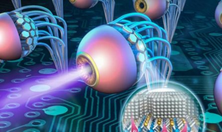
Ring resonator produced using silicon photonics and modulated internally generates a frequency ladder. Credit: Yokohama National University
The researchers produced an artificial measurement on a silicon ring resonator, utilizing the same approach used to develop complementary metal-oxide-semiconductors (CMOS), a computer chip that can save some memory. A ring resonator uses guides to control and split light waves according to particular specifications, such as specific bandwidths.
According to Baba, the silicon ring resonator photonic gadget obtained a “comb-like” optical spectra, leading to combined modes corresponding to a one-dimensional design. In other words, the gadget produced a quantifiable residential or commercial property– a synthetic measurement– that enabled the scientists to infer info about the rest of the system.
While the developed device makes up one ring, more might be stacked to waterfall effects and rapidly define optical frequency signals..
Seriously, Baba said, their platform, even with stacked rings, is much smaller sized and compact than previous approaches, which employed fiber optics connected to different parts.
” A more scalable silicon photonic chip platform offers a significant advancement, as it permits photonics with artificial dimensions to take advantage of the fully grown and sophisticated CMOS business fabrication toolbox, while also developing the methods for multi-dimensional topological phenomena to be presented into novel gadget applications,” Baba said.
The versatility of the system, consisting of the ability to reconfigure it as necessary, complements comparable static spaces in genuine area, which might help scientists bypass the dimensional restrictions of real area to comprehend phenomena even beyond 3 dimensions, according to Baba.
” This work shows the possibility that artificial and topological measurement photonics can be used practically with a silicon photonics combination platform,” Baba said. “Next, we prepare to collect all topological and artificial dimension photonic aspects to develop a topological integrated circuit.”.
Referral: “Synthetic measurement band structures on a Si CMOS photonic platform” 28 January 2022, Science Advances.DOI: 10.1126/ sciadv.abk0468.
Other contributors consist of Armandas Balčytis and Jun Maeda, Department of Electrical and Computer Engineering, Yokohama National University; Tomoki Ozawa, Advanced Institute for Materials Research, Tohoku University; and Yasutomo Ota and Satoshi Iwamoto, Institute for Nano Quantum Information Electronics, The University of Tokyo. Ota is also connected with the Department of Applied Physics and Physico-Informatics, Keio University. Iwamoto is likewise affiliated with the Research Center for Advanced Science and Technology and the Institute of Industrial Science, The University of Tokyo.
The Japan Science and Technology Agency (JPMJCR19T1, JPMJPR19L2), the Japan Society for the Promotion of Science (JP20H01845) and RIKEN supported this research study.