
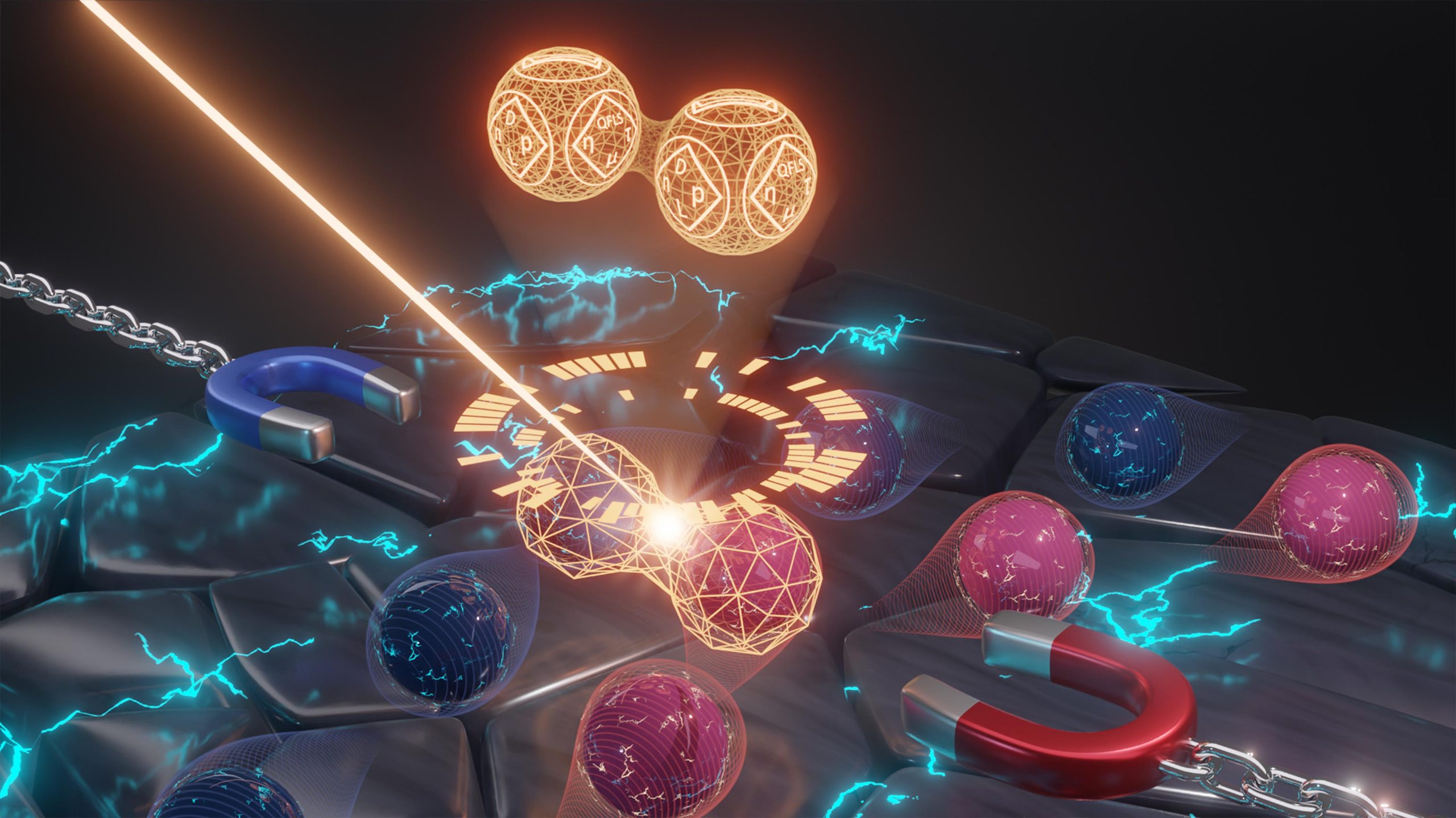
The bright spheres symbolize bound charge carriers (negative and positive) in the material. The light beam separates these charges, which are then deflected in different ways in the applied magnetic field. With the CLIMAT method, around 14 different parameters of the transport properties in semiconductors can be measured with a single measurement, for example, density, lifetime, diffusion lengths, and mobility. Credit: Laura Canil (www.canilvisuals.com)
An HZB physicist has developed a new method for the comprehensive characterization of semiconductors in a single measurement. The “Constant Light-Induced Magneto-Transport (CLIMAT)” is based on the Hall effect and allows to record 14 different parameters of transport properties of negative and positive charge carriers. The method was tested now on twelve different semiconductor materials and will save valuable time in assessing new materials for optoelectronic applications such as solar cells.
Solar cells, transistors, detectors, sensors, and LEDs all have one thing in common: they are made of semiconductor materials whose charge carriers are only released when they are hit by light (photons). The photons knock electrons (negative charge carriers) out of their orbits, which move through the material until they are captured again after a certain time. Simultaneously, holes are created in the places where the electrons are missing — these holes behave like positively charged charge carriers and are also important for the performance of the respective application.
The behavior of negative and positive charge carriers in semiconductors often differs by orders of magnitude in terms of mobility, diffusion lengths, and lifetime. Until now, the parameters of the transport properties had to be determined separately for each type of charge, using different measurement methods.
Single measurement
As part of his “Maria Skłodowska Curie Postdoctoral Fellowship,” HZB physicist Dr. Artem Musiienko has now developed a new method that can record all 14 parameters of positive and negative charge carriers in a single measurement.
The “Constant Light-Induced Magneto-Transport (CLIMAT)” uses a magnetic field vertically through the sample and a constant light source for charge separation. The charge carriers move along an electric field and are deflected by the magnetic field perpendicular to their direction of movement (Hall effect), according to their mass, mobility, and other properties.
A total of 14 different properties can be determined from the signals and, in particular, the differences between the signals of the different charge carriers, Musiienko showed with a neat little system of equations.
p and n charge carriers
“CLIMAT thus provides a comprehensive insight into the complicated mechanisms of charge transport, both positive and negative charge carriers, with a single measurement. This enables us to evaluate new types of semiconductor materials much more quickly, for example for their suitability as solar cells or for other applications,” says Musiienko.
Testing different semiconductor materials
To demonstrate the broad applicability of the new method, research teams at HZB, the University of Potsdam, and other institutions in the USA, Switzerland, the UK, and Ukraine have now used it to characterize a total of twelve very different semiconductor materials, including silicon, halide perovskite films, organic semiconductors such as Y6, semi-insulators, self-assembled monolayers, and nanoparticles. The results have now been published in Nature Communications.
Outlook: a very compact instrument
Independent experts such as Prof Vitaly Podzorov from Rutgers University, USA, awarded the CLIMAT method 15 out of 16 points in Nature Electronics and consider the new method to be groundbreaking. In particular, CLIMAT eliminates many of the steps previously required for different measurements thus saving valuable time. In early 2024, the CLIMAT method was approved for patenting by the European Patent Office under the number EP23173681.0.
“Negotiations are currently underway with companies about licensing our method,” says Musiienko. The goal is a compact measuring device, about the size of a notebook.
Reference: “Resolving electron and hole transport properties in semiconductor materials by constant light-induced magneto transport” by Artem Musiienko, Fengjiu Yang, Thomas William Gries, Chiara Frasca, Dennis Friedrich, Amran Al-Ashouri, Elifnaz Sağlamkaya, Felix Lang, Danny Kojda, Yi-Teng Huang, Valerio Stacchini, Robert L. Z. Hoye, Mahshid Ahmadi, Andrii Kanak and Antonio Abate, 5 January 2024, Nature Communications.
DOI: 10.1038/s41467-023-44418-1